

Physics of the Transistor
To the reader: Please read the “Introduction of the Physics of Electrical Circuits” written by Robert de Hilster to learn the rules of The Particle Model.
Standard Explanation
A transistor is a three-terminal electronic component that allows current to flow primarily in one direction, under the control of the base lead; and to block current flow in the opposite direction.
A transistor symbol has three connection points.
They are the Base (B), the Emitter (E) and the Collector (C).
The transistor can be used as an on/off switch or an amplifier.
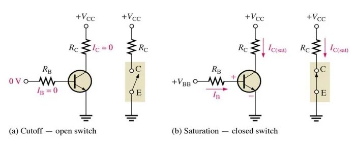
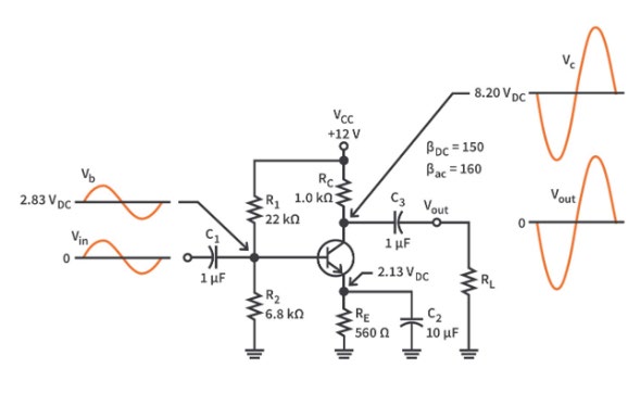
Transistor amplifier showing current flow.
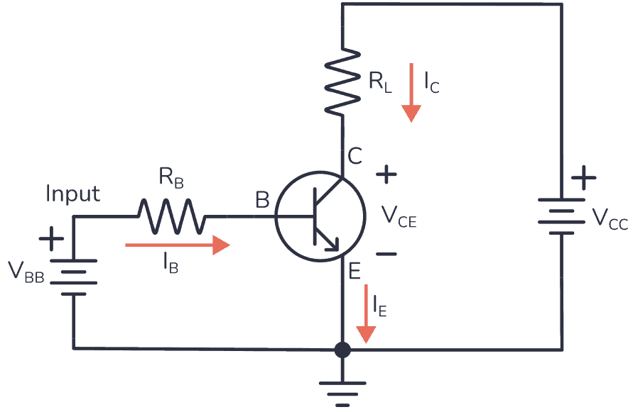
Gain of the transistor is defined as the ratio of Ic to Ib. Current is the flow of holes which is not very interesting. Instead of current, show electron (G1) flow. Figure 3 indicates that the transistor is an amplifier with ac voltage gain. What is missing in the diagram is the emitter ac voltage. The value of the emitter voltage is the sum of the collector and base voltage. The emitter voltage must be included or there is no collector current and no base current.
TPM Transistor with G1 Flow
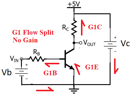
Figure 5 is The Particle Model of the transistor. G1 Particles are emitted from both batteries. They enter the emitter of the transistor as G1E (the number of G1s entering the emitter). From there G1E is split into G1B and G1C. ‘A split’ does not involve a gain.
The standard definition of gain is the ‘ratio of G1C to G1B’. So, this definition of gain is not gain; it is the ratio of the split of G1E.
Conclusion: the transistor does not have gain.
To verify, check out another drawing of transistor gain using an ac signal.
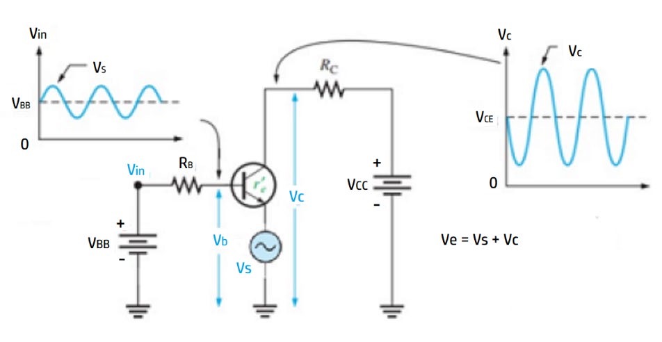
The ac source in Figure 6 is located between ground and the emitter. G1Es enter the emitter and split into Vin and Vc. Although Vc/Vin appears to show gain, they are just two arms of the emitter split. And the ratio of these two arms is not gain.
Figure 7 is the IV Curve of the Transistor.
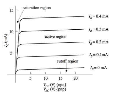
The IV curve of the transistor in Figure 7 implies that there is gain in the transistor. A base current of 0.3 mA results in a collector current of 10 mA. 10 mA / 0.3 mA results in 33.33 gain. It is true that the gain of the collector’s current matches the gain of the base current. But that only happens because the emitter current splits. The emitter current is the sum of the base current and collector current.
The graph should include the emitter current. (Graph has not been developed)
The split of the emitter current is based on the size of the collector vs the size of the base. Physically, the collector is the largest part, the base is the smallest part, and the emitter is somewhere in between. These physical sizes guarantee that the ratio of Ic to Ib is positive.
Doping
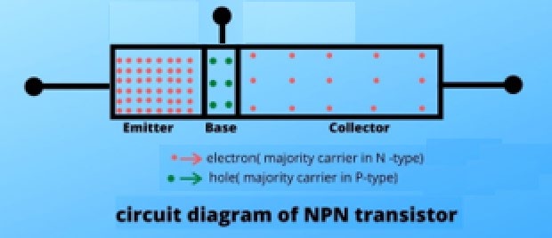
The transistor has three sections. The base has missing G1 particles (green dots), the emitter has many G1 particles (red dot), and the collector has only a few G1s.
Transistor Splitting
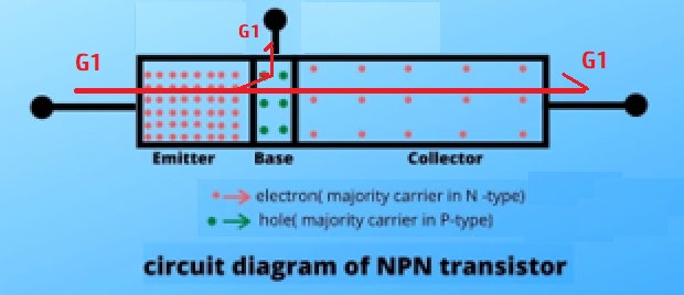
In Figure 9, the G1 particles enter the emitter from the left.
Start with a few definitions:
- G1 particle replaces the electron but has no charge.
- G1 Gravity is the random flow of G1 particles around an object (Newtonian gravity).
- Steady stream of G1 particles is current (electron flow).
- G2 particles are the orbital of a subatomic atom.
- Random flow of G2 particles around an object is the source of G2 Gravity.
- Steady stream of G2 particles is the definition of F2 force.
Explanation
The F2 force (F2M) surrounds the transistor from all directions. In most directions these forces balance out. The interesting direction is vertical. See Figure 10.
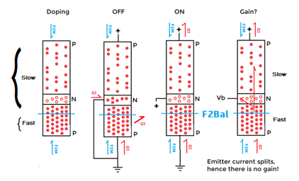
As the F2 particles move through the transistor it sets a balance point where the F2 forces meet and balance.
TPM Analysis of the Transistor
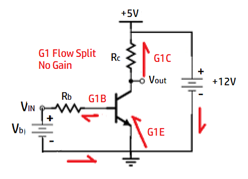
Electron flow (G1 Flow) is red. Scientists define current gain as the ratio of Ic to Ib. That ratio is clearly positive, but the ratio of the number of holes in the collector current vs the number of holes in the base current is not very interesting. It is more interesting and more realistic to define the gain in terms of electrons (G1s).
But Figure 10d shows a split of G1s, not a gain. G1 emitter flow splits into collector and base.
The gain of a transistor by normal definition is the ratio of Ic to Ib. And the ratio of that split is not a gain.
Source of the G1
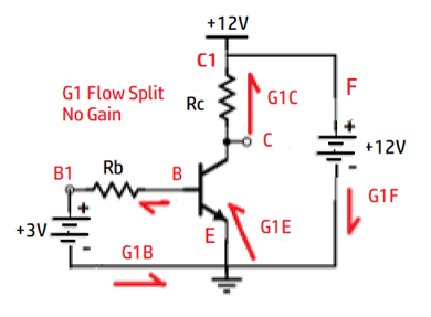
Both batteries emit G1s in proportion to their voltage rating. For example: in an interval of time, the +3V could emit 6 G1s and the +12V could emit 24 G1s. Thus, G1E would have 30 G1s in that same interval of time. For the circuit to balance and become stable, each side of the transistor must add and lose the same amount of G1s.
Finding B1 and C1 Values when Circuit is Balanced
Spreadsheet equations for base circuit (see circuit in Figure 12).
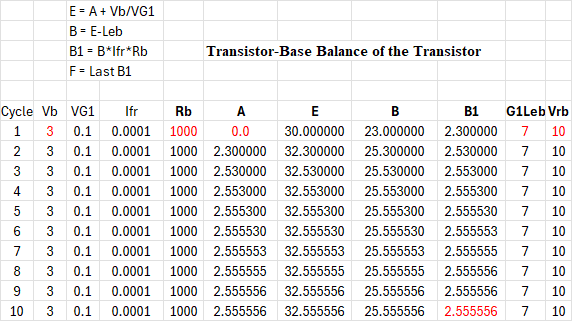
The spreadsheet of Figure 13 shows the progression of the base circuit to balance. The labels on the chart correspond to points in the circuit shown in Figure 12. Here, A is set to zero, and the chart finds the other values using the equations. Point A can be set to any value and the equations will still get the same result.
Spreadsheet equations for collector circuit (see circuit in Figure 12).
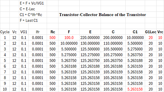
The last entries on the spreadsheet for both figures show a repeated and stable value.
