

Physics of the Diode
To the reader: Please read the “Introduction of the Physics of Electrical Circuits” written by Robert de Hilster to learn the rules about The Particle Model.
A diode is a two-terminal electronic component that allows current to flow primarily in one direction, making it essential for controlling electrical circuits.
A diode symbol is shown in Figure 1.

Besides the junction diode there are many more types.
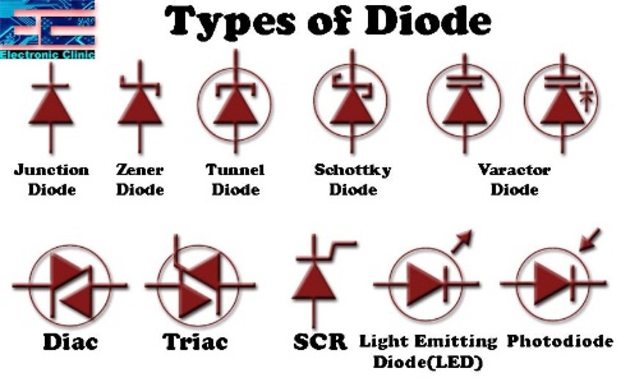
However, only the junction diode is explained in this document. The junction diode symbol has two sections. The positive terminal is shown with a triangle while the negative terminal is shown with a straight line. The diode conducts current in the direction of the triangle (P→N). The diode blocks current in the reverse direction (N→P). Electron flow moves in the opposite direction. Therefore, electron flow is in the (N→P) direction while the electrons are blocked in the (P→N) direction.
Figure 3 is the IV Curve of the Diode.

There are two knees on the IV Curve of the diode. The first knee is in the first quadrant and represents the forward bias or the conduction of current. The second knee is in the third quadrant and represents the reverse bias of the diode or the loss of conduction.
Standard Explanation of the Diode
A diode is defined as an electronic device that conducts electricity only in one direction. It consists of two terminals: the anode and the cathode. When the anode is at a higher voltage than the cathode (forward bias), the diode allows current to flow. Conversely, when the cathode is at a higher voltage (reverse bias), the diode blocks current flow.

Depletion Layer

Figure 5 explains the diode based on the size of the depletion layer. The depletion layer is neutral when there is no voltage applied. See Figure 5a. The layer is decreased when the diode is forward biased and allows the electron to flow through the diode. The layer is increased when the diode is reversed biased and so no current flows. This explanation is based on charge. The Particle Model rejects charge and therefore rejects the concept of a depletion layer.
The Particle Model (TPM) Explanation
TPM does not use current to describe the physicality of the diode. ‘Current’ is the flow of holes and TPM does not find that very interesting. TPM used the flow of G1s (electrons with no charge) which are clearly physical. Figure 6 shows how the diode is doped. This figure is based on the added or missing electrons (red dots are the electrons or G1 particles).
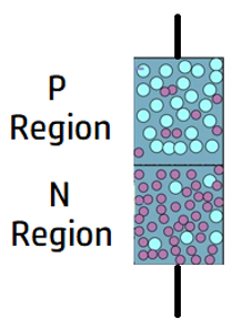
The red dots in Figure 6 are atoms with extra electrons (G1s). The blue dots are the atoms with a missing G1. The N Region has more G1s than the P Region. It is this unbalanced configuration that allows current to flow in one direction and block current in the reverse direction.
Start with a few definitions:
- G1 particle replaces the electron but has no charge.
- G1 Gravity is the random flow of G1 particles around an object (Newtonian gravity).
- Steady stream of G1 particles is current (electron flow).
- G2 particles are the orbital of a subatomic atom.
- Random flow of G2 particles around an object is the source of G2 Gravity.
- Steady stream of G2 particles is the definition of F2 force.
A diode is a two-terminal electronic component that allows current to flow primarily in one direction (forward biased) and blocks current flow in the opposite direction (reverse biased). See Figure 7.

Doping
The diode has two regions. The P region with very few G1 Particles and the N region with many G1 particles. The ‘F2 Bal’ line is located where the number of G1s (red dot) above the line matches the number of G1s below the line. The light blue circles are empty spaces. It is this imbalance that allows the diode to be used as a conductor or as a nonconductor.
Definition: F2 Force — G2 particles organized around an object setting up F2 forces that push to the center of mass of the object.
The F2 force surrounds the diode from all directions. In most directions these forces balance out. The interesting direction is through the top and from the bottom. See Figure 7. As the F2 particles move through the diode it sets a balance point where the F2 forces meet and balance. The ‘F2 Bal’ is identified by a blue line. In Figure 7, there are the same number of G1s above and below the line.
Forward Biased

The G2 force of gravity (F2) surrounds the diode in all directions. The diode is doped so that there are more G1s in the N region than in the P region. Because of this imbalance, the F2 force is equal at the blue line (F2 Bal) in Figure 8.
This offset is what gives the diode the ability to aid the forward current and block the reversed current.
Figure 8 shows the G1 particle flow through the diode as red arrows entering the N Region. Even though there is very little open space the F2 force is strong enough to accelerate the G1s through the N Region and to keep it going all the way through.
Reversed Biased

Figure 9 shows the diode in the reverse biased mode. In this case the G1 particles enter the P region aided by the downward F2 force.
The G1 particle accelerates until it hits the F2 Bal point. After the F2 Bal the opposing F2 force (upward) is very strong and slows the speed of the G1 particle. This strong F2 force prevents the G1 from passing all the way through. Both the G1 flow (red) and the current flow (black) are blocked past the ‘F2 Bal’ line.
What causes the diode IV curve to change direction at the knee?

Speed
When the forward IV curve reaches the knee, it changes direction. At this point the current also increases. An increase of the number of G1s flowing in the diode causes the F2 force around the diode to increase. This increased F2 force causes the G1s to increase their speed. The faster the G1s go, the more easily they pass through the diode. So, fewer G1s are lost and the voltage drop increases but at a slower rate.
The vertical IV curve in the first quadrant indicates that the G1s are moving faster; they cause less G1 loss (voltage loss) because the G1 Flow (electron flow) is increasing. A faster G1 will easily pass through the diode. A slower G1 will be attracted to the atoms of the diode.
Knee Voltage
Why does the diode IV Curve show a low current before the knee and then increase after the knee?
At low current, the F2 force around the diode is small. Since F2 is small, it does not have the force to push the G1s through the diode and out. This is because there is a high density of G1s in the N Region of the diode and needs a strong F2 to get them through. A few of the G1s that make it through gives the diode a very small current as the voltage approaches the knee.
The current increases after the knee. When the current increases, the F2 force increases and the diode conducts. That is, the G1s easily pass through the diode.
The Third Quadrant
It is interesting to note that a second knee occurs in the third quadrant. As the reverse current increases, the F2 force increases and the diode reaches the avalanche or breakdown region.
